- 您现在的位置:买卖IC网 > Sheet目录2008 > MAX1308ECM+T (Maxim Integrated Products)IC ADC 12BIT 8CH 4MSPS 48LQFP
MAX1304–MAX1306/MAX1308–MAX1310/MAX1312–MAX1314
8-/4-/2-Channel, 12-Bit, Simultaneous-Sampling ADCs
with ±10V, ±5V, and 0 to +5V Analog Input Ranges
______________________________________________________________________________________
13
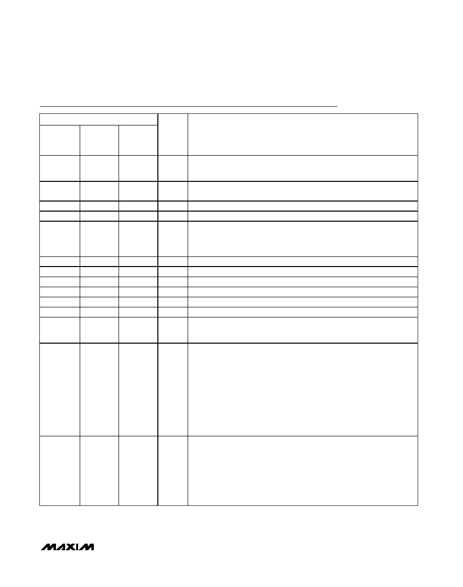
Pin Description
PIN
MAX1304
MAX1308
MAX1312
MAX1305
MAX1309
MAX1313
MAX1306
MAX1310
MAX1314
NAME
FUNCTION
1, 15, 17
AVDD
Analog Power Input. AVDD is the power input for the analog section of the
converter. Apply +5V to AVDD. Connect all AVDD pins together. See the
Layout, Grounding, and Bypassing section for additional information.
2, 3, 14,
16, 23
2, 3, 14,
16, 23
2, 3, 14,
16, 23
AGND
Analog Ground. AGND is the power return for AVDD. Connect all AGND
pins together.
4
CH0
Channel 0 Analog Input
5
CH1
Channel 1 Analog Input
66
6
MSV
Midscale Voltage Bypass. For the unipolar MAX1304/MAX1305/MAX1306,
connect a 2.2F and a 0.1F capacitor from MSV to AGND. For the bipolar
MAX1308/MAX1309/MAX1310/MAX1312/MAX1313/MAX1314, connect
MSV to AGND.
7
—
CH2
Channel 2 Analog Input
8
—
CH3
Channel 3 Analog Input
9
—
CH4
Channel 4 Analog Input
10
—
CH5
Channel 5 Analog Input
11
—
CH6
Channel 6 Analog Input
12
—
CH7
Channel 7 Analog Input
13
INTCLK/
EXTCLK
Clock-Mode Select Input. Connect INTCLK/EXTCLK to AVDD to select the
internal clock. Connect INTCLK/EXTCLK to AGND to use an external clock
connected to CLK.
18
REFMS
Midscale Reference Bypass or Input. REFMS connects through a 5k_ resistor to
the internal +2.5V bandgap reference buffer.
For the MAX1304/MAX1305/MAX1306 unipolar devices, VREFMS is the input to
the unity-gain buffer that drives MSV. MSV sets the midpoint of the input voltage
range. For internal reference operation, bypass REFMS with a ≥ 0.01F
capacitor to AGND. For external reference operation, drive REFMS with an
external voltage from +2V to +3V.
For the MAX1308/MAX1309/MAX1310/MAX1312/MAX1313/MAX1314 bipolar
devices, connect REFMS to REF. For internal reference operation, bypass the
REFMS/REF node with a ≥ 0.01F capacitor to AGND. For external reference
operation, drive the REFMS/REF node with an external voltage from +2V to +3V.
19
REF
ADC Reference Bypass or Input. REF connects through a 5k_ resistor to the
internal +2.5V bandgap reference buffer.
For internal reference operation, bypass REF with a ≥ 0.01F capacitor.
For external reference operation with the MAX1304/MAX1305/MAX1306
unipolar devices, drive REF with an external voltage from +2V to +3V.
For external reference operation with the MAX1308/MAX1309/MAX1310/
MAX1312/MAX1313/MAX1314 bipolar devices, connect REFMS to REF and
drive the REFMS/REF node with an external voltage from +2V to +3V.
发布紧急采购,3分钟左右您将得到回复。
相关PDF资料
MAX1320ECM+T
IC ADC 14BIT 8CH 2MSPS 48LQFP
MAX132EWG+T
IC ADC 18BIT SERIAL 24-SOIC
MAX135EPI+
IC ADC 15BIT PARALLEL 28-DIP
MAX1361MEUB+T
IC SYSTEM MON 10BIT 4CH 10-UMAX
MAX1364MEUB+T
IC SYSTEM MON 12BIT 4CH 10-UMAX
MAX1394ETB+T
IC ADC 8BIT 416KSPS 10-TDFN-EP
MAX1395ETB+T
IC ADC 10BIT 357KSPS 10-TDFN
MAX1400CAI+
IC ADC 18BIT LP 28-SSOP
相关代理商/技术参数
MAX1308ECM-T
功能描述:模数转换器 - ADC RoHS:否 制造商:Texas Instruments 通道数量:2 结构:Sigma-Delta 转换速率:125 SPs to 8 KSPs 分辨率:24 bit 输入类型:Differential 信噪比:107 dB 接口类型:SPI 工作电源电压:1.7 V to 3.6 V, 2.7 V to 5.25 V 最大工作温度:+ 85 C 安装风格:SMD/SMT 封装 / 箱体:VQFN-32
MAX1308EVB16
功能描述:数据转换 IC 开发工具 MAX1308 Evaluation Kit/Evaluation System RoHS:否 制造商:Texas Instruments 产品:Demonstration Kits 类型:ADC 工具用于评估:ADS130E08 接口类型:SPI 工作电源电压:- 6 V to + 6 V
MAX1308EVKIT
功能描述:数据转换 IC 开发工具 MAX1308 Evaluation Kit/Evaluation System RoHS:否 制造商:Texas Instruments 产品:Demonstration Kits 类型:ADC 工具用于评估:ADS130E08 接口类型:SPI 工作电源电压:- 6 V to + 6 V
MAX1309ECM
功能描述:模数转换器 - ADC RoHS:否 制造商:Texas Instruments 通道数量:2 结构:Sigma-Delta 转换速率:125 SPs to 8 KSPs 分辨率:24 bit 输入类型:Differential 信噪比:107 dB 接口类型:SPI 工作电源电压:1.7 V to 3.6 V, 2.7 V to 5.25 V 最大工作温度:+ 85 C 安装风格:SMD/SMT 封装 / 箱体:VQFN-32
MAX1309ECM/V+
功能描述:模数转换器 - ADC 12-Bit 4Ch 1.075Msps 3V Precision ADC RoHS:否 制造商:Texas Instruments 通道数量:2 结构:Sigma-Delta 转换速率:125 SPs to 8 KSPs 分辨率:24 bit 输入类型:Differential 信噪比:107 dB 接口类型:SPI 工作电源电压:1.7 V to 3.6 V, 2.7 V to 5.25 V 最大工作温度:+ 85 C 安装风格:SMD/SMT 封装 / 箱体:VQFN-32
MAX1309ECM/V+T
功能描述:模数转换器 - ADC 12-Bit 4Ch 1.075Msps 3V Precision ADC RoHS:否 制造商:Texas Instruments 通道数量:2 结构:Sigma-Delta 转换速率:125 SPs to 8 KSPs 分辨率:24 bit 输入类型:Differential 信噪比:107 dB 接口类型:SPI 工作电源电压:1.7 V to 3.6 V, 2.7 V to 5.25 V 最大工作温度:+ 85 C 安装风格:SMD/SMT 封装 / 箱体:VQFN-32
MAX1309ECM+
功能描述:模数转换器 - ADC 12-Bit 4Ch 1.075Msps 3V Precision ADC RoHS:否 制造商:Texas Instruments 通道数量:2 结构:Sigma-Delta 转换速率:125 SPs to 8 KSPs 分辨率:24 bit 输入类型:Differential 信噪比:107 dB 接口类型:SPI 工作电源电压:1.7 V to 3.6 V, 2.7 V to 5.25 V 最大工作温度:+ 85 C 安装风格:SMD/SMT 封装 / 箱体:VQFN-32
MAX1309ECM+T
功能描述:模数转换器 - ADC 12-Bit 4Ch 1.075Msps 3V Precision ADC RoHS:否 制造商:Texas Instruments 通道数量:2 结构:Sigma-Delta 转换速率:125 SPs to 8 KSPs 分辨率:24 bit 输入类型:Differential 信噪比:107 dB 接口类型:SPI 工作电源电压:1.7 V to 3.6 V, 2.7 V to 5.25 V 最大工作温度:+ 85 C 安装风格:SMD/SMT 封装 / 箱体:VQFN-32